#VHDL modeling
Explore tagged Tumblr posts
Visit Tumblr Blog
Explore Tumblr blogs with no restrictions, modern design and the best experience.
Last Seen Tumblr Blogs


Fun Fact
70% of Tumblr users say the Dashboard is their favorite place to spend time online.
Text
youtube
VHDL Basics : Begin the World of FPGA Design Tools & VHDL Design Flow
Welcome to our comprehensive guide on FPGA design tools and VHDL design flow! In this video, we dive into the fascinating world of FPGA design and explore the essential tools and methodologies needed for successful FPGA development. Whether you're a beginner or an experienced engineer, this tutorial will provide valuable insights and tips to enhance your FPGA design skills. We start by introducing the fundamentals of FPGA design, explaining the benefits and versatility of using FPGAs in various applications. From there, we explore the wide range of design tools available, from popular industry-standard software like Xilinx Vivado and Altera Quartus Prime to open-source alternatives like GHDL and Icarus Verilog. We highlight the strengths and features of each toolset, enabling you to choose the most suitable one for your projects. With a solid foundation in FPGA design and tools, we then delve into the VHDL (VHSIC Hardware Description Language) design flow. From understanding the basics of VHDL syntax to implementing complex digital designs, we provide step-by-step explanations and practical demonstrations. You'll learn about entity and architecture design, the importance of libraries, and how to simulate and synthesize VHDL code for your FPGA. To ensure a holistic learning experience, we discuss common challenges and pitfalls in FPGA design and provide valuable troubleshooting tips. We also touch upon advanced topics like FPGA optimization techniques, timing analysis, and physical implementation considerations. So, whether you're a student, hobbyist, or professional looking to enhance your FPGA design skills, this tutorial is the ultimate resource to get started on your journey. Join us now and unlock the vast potential of FPGA design tools and the VHDL design flow! FPGA design tools, VHDL design flow, FPGA development, Xilinx Vivado, Altera Quartus Prime, VHDL, Verilog, VHDL syntax, digital design, entity architecture, libraries, simulate VHDL code, synthesize VHDL code, FPGA optimization techniques, timing analysis, physical implementation, FPGA design skills.
Subscribe to "Learn And Grow Community"
YouTube : https://www.youtube.com/@LearnAndGrowCommunity
LinkedIn Group : https://www.linkedin.com/groups/7478922/
Blog : https://LearnAndGrowCommunity.blogspot.com/
Facebook : https://www.facebook.com/JoinLearnAndGrowCommunity/
Twitter Handle : https://twitter.com/LNG_Community
DailyMotion : https://www.dailymotion.com/LearnAndGrowCommunity
Instagram Handle : https://www.instagram.com/LearnAndGrowCommunity/
Follow #LearnAndGrowCommunity
#HDL Design#Digital Design#Verilog#VHDL#FPGA#Simulation#Synthesis#B.Tech#VLSI#Training#Career#ASIC#Xilinx#Students#hardware description language#VHDL tutorial#VHDL beginner guide#VHDL syntax#VHDL data types#VHDL modeling#behavioral modeling#data flow modeling#FSM#FPGA design tools#VHDL design flow#FPGA development#Xilinx Vivado#Altera Quartus Prime#entity#architecture
1 note
·
View note
Text
Understanding FPGA Architecture: Key Insights
Introduction to FPGA Architecture
Imagine having a circuit board that you could rewire and reconfigure as many times as you want. This adaptability is exactly what FPGAs offer. The world of electronics often seems complex and intimidating, but understanding FPGA architecture is simpler than you think. Let’s break it down step by step, making it easy for anyone to grasp the key concepts.
What Is an FPGA?
An FPGA, or Field Programmable Gate Array, is a type of integrated circuit that allows users to configure its hardware after manufacturing. Unlike traditional microcontrollers or processors that have fixed functionalities, FPGAs are highly flexible. You can think of them as a blank canvas for electrical circuits, ready to be customized according to your specific needs.
How FPGAs Are Different from CPUs and GPUs
You might wonder how FPGAs compare to CPUs or GPUs, which are more common in everyday devices like computers and gaming consoles. While CPUs are designed to handle general-purpose tasks and GPUs excel at parallel processing, FPGAs stand out because of their configurability. They don’t run pre-defined instructions like CPUs; instead, you configure the hardware directly to perform tasks efficiently.
Basic Building Blocks of an FPGA
To understand how an FPGA works, it’s important to know its basic components. FPGAs are made up of:
Programmable Logic Blocks (PLBs): These are the “brains” of the FPGA, where the logic functions are implemented.
Interconnects: These are the wires that connect the logic blocks.
Input/Output (I/O) blocks: These allow the FPGA to communicate with external devices.
These elements work together to create a flexible platform that can be customized for various applications.
Understanding Programmable Logic Blocks (PLBs)
The heart of an FPGA lies in its programmable logic blocks. These blocks contain the resources needed to implement logic functions, which are essentially the basic operations of any electronic circuit. In an FPGA, PLBs are programmed using hardware description languages (HDLs) like VHDL or Verilog, enabling users to specify how the FPGA should behave for their particular application.
What are Look-Up Tables (LUTs)?
Look-Up Tables (LUTs) are a critical component of the PLBs. Think of them as small memory units that can store predefined outputs for different input combinations. LUTs enable FPGAs to quickly execute logic operations by “looking up” the result of a computation rather than calculating it in real-time. This speeds up performance, making FPGAs efficient at performing complex tasks.
The Role of Flip-Flops in FPGA Architecture
Flip-flops are another essential building block within FPGAs. They are used for storing individual bits of data, which is crucial in sequential logic circuits. By storing and holding values, flip-flops help the FPGA maintain states and execute tasks in a particular order.
Routing and Interconnects: The Backbone of FPGAs
Routing and interconnects within an FPGA are akin to the nervous system in a human body, transmitting signals between different logic blocks. Without this network of connections, the logic blocks would be isolated and unable to communicate, making the FPGA useless. Routing ensures that signals flow correctly from one part of the FPGA to another, enabling the chip to perform coordinated functions.
Why are FPGAs So Versatile?
One of the standout features of FPGAs is their versatility. Whether you're building a 5G communication system, an advanced AI model, or a simple motor controller, an FPGA can be tailored to meet the exact requirements of your application. This versatility stems from the fact that FPGAs can be reprogrammed even after they are deployed, unlike traditional chips that are designed for one specific task.
FPGA Configuration: How Does It Work?
FPGAs are configured through a process called “programming” or “configuration.” This is typically done using a hardware description language like Verilog or VHDL, which allows engineers to specify the desired behavior of the FPGA. Once programmed, the FPGA configures its internal circuitry to match the logic defined in the code, essentially creating a custom-built processor for that particular application.
Real-World Applications of FPGAs
FPGAs are used in a wide range of industries, including:
Telecommunications: FPGAs play a crucial role in 5G networks, enabling fast data processing and efficient signal transmission.
Automotive: In modern vehicles, FPGAs are used for advanced driver assistance systems (ADAS), real-time image processing, and autonomous driving technologies.
Consumer Electronics: From smart TVs to gaming consoles, FPGAs are used to optimize performance in various devices.
Healthcare: Medical devices, such as MRI machines, use FPGAs for real-time image processing and data analysis.
FPGAs vs. ASICs: What’s the Difference?
FPGAs and ASICs (Application-Specific Integrated Circuits) are often compared because they both offer customizable hardware solutions. The key difference is that ASICs are custom-built for a specific task and cannot be reprogrammed after they are manufactured. FPGAs, on the other hand, offer the flexibility of being reconfigurable, making them a more versatile option for many applications.
Benefits of Using FPGAs
There are several benefits to using FPGAs, including:
Flexibility: FPGAs can be reprogrammed even after deployment, making them ideal for applications that may evolve over time.
Parallel Processing: FPGAs excel at performing multiple tasks simultaneously, making them faster for certain operations than CPUs or GPUs.
Customization: FPGAs allow for highly customized solutions, tailored to the specific needs of a project.
Challenges in FPGA Design
While FPGAs offer many advantages, they also come with some challenges:
Complexity: Designing an FPGA requires specialized knowledge of hardware description languages and digital logic.
Cost: FPGAs can be more expensive than traditional microprocessors, especially for small-scale applications.
Power Consumption: FPGAs can consume more power compared to ASICs, especially in high-performance applications.
Conclusion
Understanding FPGA architecture is crucial for anyone interested in modern electronics. These devices provide unmatched flexibility and performance in a variety of industries, from telecommunications to healthcare. Whether you're a tech enthusiast or someone looking to learn more about cutting-edge technology, FPGAs offer a fascinating glimpse into the future of computing.
2 notes
·
View notes
Text
Mastering VLSI: Why the Right Training Matters for a Thriving Tech Career
The Rising Demand for VLSI Experts The modern world is driven by electronics. From smartphones to smart cars, every innovation depends on microchips designed using VLSI (Very Large Scale Integration) technology. With the growing use of AI, IoT, and automation, the need for skilled VLSI professionals has increased rapidly. This makes VLSI an essential field for those looking to build a strong career in electronics and semiconductor industries. Choosing the right learning path is key to making the most of this opportunity.
Exploring the Benefits of VLSI Online Training Courses Many learners today seek flexible and effective ways to upskill. VLSI online training courses offer an excellent solution by combining convenience with quality education. These courses provide access to experienced instructors, practical assignments, and industry-based projects—all from the comfort of home. Learners can grasp digital design, physical design, verification, and ASIC/FPGA concepts without sacrificing their job or academic responsibilities. The online model also allows repeated learning and flexible scheduling, making it ideal for beginners as well as professionals wanting to upgrade their knowledge.
Choosing the Right Learning Mode While online learning provides flexibility, some individuals prefer classroom-based teaching for real-time interaction and immediate doubt clearing. The choice between online and offline modes largely depends on individual preferences, learning habits, and career goals. However, what truly matters is the quality of the training and the expertise of the instructors involved.
Key Skills Taught in VLSI Training A well-structured VLSI course should cover areas like CMOS technology, HDL languages such as Verilog and VHDL, physical design flow, and functional verification techniques. Practical exposure through lab sessions or simulation tools is crucial. Additionally, learners should be guided on real-time projects to apply their theoretical knowledge to industry problems.
Why VLSI Coaching in Hyderabad is Gaining Popularity Hyderabad has become a major hub for semiconductor and electronics industries. As a result, VLSI coaching in Hyderabad has gained recognition for producing skilled professionals. Reputed training centers in the city offer tailored coaching with an industry-aligned curriculum, experienced faculty, and placement support. Many aspirants from across the country travel to Hyderabad to benefit from this coaching environment that bridges academic learning with industry demands.
Conclusion VLSI technology plays a vital role in shaping the electronics and semiconductor industries. Whether through VLSI online training courses or classroom-based programs like VLSI coaching in Hyderabad, acquiring the right skills is essential for career growth. Institutions like Takshila Institute of VLSI Technologies provide training that matches industry standards, helping learners succeed in a competitive field. The choice of platform and location may differ, but the goal remains the same—building a strong foundation in VLSI for a successful future.
0 notes
Text
Why Is Electronics and Communication Engineering in Hyderabad Ideal for Aspiring Engineers?

Electronics and Communication Engineering (ECE) has long been regarded as one of the most versatile and in-demand engineering disciplines in India and globally. Among the many cities offering high-quality education in ECE, Hyderabad stands out due to its strong academic infrastructure, flourishing tech industry, and dynamic learning environment. For students looking to pursue Electronics and Communication Engineering in Hyderabad, institutions like HITAM (Hyderabad Institute of Technology and Management) offer a holistic and industry-relevant curriculum that equips graduates with the skills to thrive in today’s competitive landscape.
In this post, we’ll explore why Hyderabad, particularly HITAM, is becoming a hotspot for ECE education.
Why Choose Electronics and Communication Engineering?
Before diving into Hyderabad-specific advantages, it’s important to understand the appeal of ECE as a career path.
ECE blends principles of electrical engineering and computer science, offering a wide scope in sectors such as:
- Telecommunications
- Embedded Systems
- Signal Processing
- Consumer Electronics
- Robotics and Automation
- Semiconductor Industry
- IoT (Internet of Things)
- AI and Machine Learning
Graduates can work as design engineers, communication analysts, embedded systems developers, or research scientists in the public and private sectors.
Why Hyderabad for ECE?
Hyderabad has become a tech powerhouse in India, with a thriving ecosystem of IT parks, electronics manufacturing hubs, and R&D centers. The city’s growth in these sectors directly complements ECE students' training.
Here are some compelling reasons to study Electronics and Communication Engineering in Hyderabad:
1) Thriving Tech Ecosystem: Hyderabad is home to major global and Indian tech giants like Qualcomm, Intel, Microsoft, and TCS. These companies actively recruit engineering graduates, especially those with a background in ECE.
2) Startup Culture: The city has a robust startup ecosystem, supported by initiatives like T-Hub and WE-Hub. ECE students interested in entrepreneurship find Hyderabad to be a nurturing ground for innovation and prototyping.
3) Academic Excellence: Institutes like HITAM are leading the way in providing a future-ready engineering education. HITAM, in particular, emphasizes experiential learning, industry internships, and research-focused study, preparing students for both jobs and higher education.
4) Smart City Advantage: Hyderabad is rapidly transforming into a smart city, with IoT-based urban infrastructure and smart grids—areas directly related to ECE. Students gain practical exposure to these developments, enhancing real-world learning.
Why HITAM for Electronics and Communication Engineering?
HITAM is a NAAC-accredited institution and an emerging name among the top engineering colleges in Hyderabad. It offers a highly relevant and innovative ECE program integrating academic knowledge with practical application.
Let’s look at the factors that set HITAM apart:
1) Outcome-Based Education: HITAM follows a strong Outcome-Based Education (OBE) model aligned with NBA accreditation standards. This approach ensures that students graduate with demonstrable problem-solving, innovation, and project management skills.
2) Industry-Aligned Curriculum: HITAM’s ECE curriculum is frequently updated in collaboration with industry experts. Students are trained in modern tools like MATLAB, VHDL, Python, and machine learning technologies relevant to ECE.
3) Project-Based Learning: HITAM emphasizes hands-on, project-based learning (PBL). Students work on real-world problems, sometimes collaborating with industry partners, building portfolios that make them job-ready.
4) Advanced Laboratories: HITAM boasts state-of-the-art labs for embedded systems, digital signal processing, IoT, and VLSI design. These labs provide a rich environment for experimentation, prototyping, and research.
5) Research and Innovation: HITAM encourages undergraduate research through its Innovation & Entrepreneurship Development Cell (IEDC). ECE students regularly participate in hackathons, publish papers, and receive funding for tech innovations.
6) Placement Support: HITAM has a strong placement cell with established links to the electronics and IT industries. Students from the ECE stream have secured roles in companies like Infosys, Capgemini, Tech Mahindra, and startups working in IoT and automation.
7) Ethical and Sustainable Learning: In addition to technical excellence, HITAM instills sustainability, ethics, and leadership values—essential traits in today’s engineering landscape.
Future Scope for ECE Graduates from Hyderabad
Graduating with an ECE degree from Hyderabad opens doors in multiple industries. Some of the future-focused roles include:
- AI Hardware Engineer
- Communication Network Designer
- IoT Systems Architect
- Embedded System Developer
- VLSI Chip Designer
- Wireless Protocol Engineer
The Indian government’s push for "Make in India" and Digital India has further boosted the demand for skilled ECE professionals, particularly in electronics design and manufacturing.
Additionally, Hyderabad’s expanding aerospace, defense, and smart manufacturing sectors seek professionals with ECE expertise.
Conclusion
Studying Electronics and Communication Engineering in Hyderabad is a smart decision for any engineering aspirant. With its vibrant tech ecosystem, high-quality academic institutions like HITAM, and strong industry collaboration, Hyderabad provides everything a student needs to grow into a competent and successful ECE professional.
If you’re passionate about blending technology with communication systems, innovating solutions, and working on cutting-edge technologies, pursuing ECE at an institution like HITAM will give you the strong foundation and exposure you need.
Explore HITAM’s ECE program and take your first step toward a future in advanced electronics and communication. 👉 Visit: https://hitam.org/electronics-and-communication-engineering/ to learn more.
0 notes
Text
CSU22022 Project 2 MICROCODED INSTRUCTION SET PROCESSOR
Description: The second project will implement a Microprogrammed Instruction Set Processor. This builds on the VHDL model from the first project. The following modifications are required: Increase the number of registers in the register-file from 32 to 33. This requires an additional select bit for the two multiplexers (Bus A and Bus B) and the destination decoder. These are separate signals (TD,…
0 notes
Text
Smart Datasheet- AI Smart Datasheet- Smart Datasheet Tool

Discover Smart Datasheet - the ultimate AI-powered tool for creating and managing smart datasheets effortlessly. Enhance productivity with intelligent automation and seamless data. Extract C/C++, IP-XACT, UVM, Verilog, VHDL, SystemRDL, JSON, YAML models or formats from PDF datasheets. In semiconductor engineering, Intellectual Property (IP) forms the building blocks for System-on-Chip (SoC). The numerous providers distribute datasheets in PDF format which need to be understood and new models created. The manual model creation process is error-prone and tedious which creates needless risk for the development of the SoC.
All this can be automated using Smart Datasheet which transforms a PDF IP into a model for downstream consumption by the SoC development team. It uses state-of-the-art AI engines to extract the relevant information from the PDF files, then it uses Agnisys’ IDesignSpec to create the models. Word files dumped into PDF are also possible to be ingested.
The Smart Datasheet website helps the user create models quickly from the existing datasheets. It helps the SoC developers automatically create accurate models that enable them to go-to-market faster and with high quality.
1 note
·
View note
Text
ASIC Design of Complex Multiplier: A Comprehensive Overview

In the modern era of digital signal processing (DSP) and communication systems, multipliers play a pivotal role. Complex multipliers, in particular, are essential in a wide array of applications such as Fast Fourier Transforms (FFT), Digital Down Converters (DDC), and MIMO communication systems. The design of an Application-Specific Integrated Circuit (ASIC) for a complex multiplier presents unique challenges and opportunities. In this blog, we delve into the intricacies of ASIC design for complex multipliers, exploring their architecture, design methodologies, and optimization techniques.
What is a Complex Multiplier?
A complex multiplier is a circuit that performs multiplication of two complex numbers. Mathematically, if and are two complex numbers, their product is given by:
This equation shows that a complex multiplier requires four real multiplications and two real additions/subtractions.
Key Considerations in ASIC Design of Complex Multipliers
Area Efficiency: ASIC designs often operate under strict area constraints. Optimizing the layout and minimizing the number of logic gates are crucial for reducing silicon area.
Power Consumption: Power efficiency is paramount, especially for portable or battery-operated devices. Techniques like clock gating, operand isolation, and optimized arithmetic circuits help in reducing dynamic and static power consumption.
Speed: High-speed operation is critical for real-time applications. The multiplier design must ensure minimal propagation delay while maintaining accuracy.
Precision: Depending on the application, the design may require fixed-point or floating-point arithmetic, which significantly impacts complexity and performance.
Process Technology: The choice of CMOS technology node (e.g., 28nm, 14nm, etc.) influences performance, power, and area (PPA) trade-offs.
Architecture of a Complex Multiplier
A typical complex multiplier architecture consists of the following components:
Four Real Multipliers: These are the core computation units.
Two Adders/Subtractors: These units perform the addition and subtraction of intermediate results.
Pipeline Registers (Optional): Pipelining enhances throughput by reducing the critical path.
To optimize the design, advanced techniques such as Booth encoding, Wallace tree structures, or Distributed Arithmetic (DA) can be employed for the real multipliers.
Design Methodology
Behavioral Modeling: The initial design begins with a high-level behavioral model in languages like VHDL or Verilog.
Synthesis: The behavioral model is synthesized into a gate-level netlist using ASIC synthesis tools like Synopsys Design Compiler.
Place and Route (P&R): The synthesized netlist is mapped to physical silicon, ensuring minimal area and optimal routing.
Timing Analysis: Static Timing Analysis (STA) is conducted to ensure the design meets timing constraints.
Power Analysis: Tools like PrimePower are used to estimate dynamic and leakage power.
Verification: Functional and formal verification ensure the design adheres to the specification.
Optimization Techniques
Shared Multipliers: Sharing multiplier resources between multiple computations can significantly reduce area and power.
Approximate Computing: For applications tolerant to small errors, approximate multipliers can be used to save power and area.
Parallel Processing: Increasing parallelism can improve throughput but must be balanced against area and power constraints.
Custom Arithmetic Units: Designing custom arithmetic circuits tailored to specific applications can yield significant gains in efficiency.
Challenges in ASIC Design
Design Complexity: Managing trade-offs between speed, power, and area is challenging, particularly in advanced nodes.
Process Variability: Variations in the manufacturing process can impact performance and yield.
Integration: The multiplier must seamlessly integrate with other blocks in the ASIC.
Applications of Complex Multipliers
Signal Processing: Used in FFTs, FIR filters, and spectral analysis.
Wireless Communication: Essential for modulation and demodulation tasks.
Image Processing: Facilitates convolution and correlation operations.
Cryptography: Key component in algorithms like RSA and ECC.
Conclusion
The ASIC design of a complex multiplier is a multifaceted process requiring careful consideration of performance, power, and area trade-offs. With advancements in process technology and design tools, engineers can achieve highly efficient designs tailored to specific applications. By leveraging optimization techniques and innovative architectures, complex multipliers can continue to meet the growing demands of modern DSP and communication systems.
Whether you're a seasoned ASIC designer or a budding engineer, the design of a complex multiplier offers an exciting opportunity to push the boundaries of silicon design and computational efficiency.
#Top Most ASIC companies in India#Famous ASIC companies in Bengaluru#Best ASIC companies in USA#Most Famous companies in Hyderabad
0 notes
Text
Understanding FPGA Architecture: Key Insights
Introduction to FPGA Architecture
Imagine having a circuit board that you could rewire and reconfigure as many times as you want. This adaptability is exactly what FPGAs offer. The world of electronics often seems complex and intimidating, but understanding FPGA architecture is simpler than you think. Let’s break it down step by step, making it easy for anyone to grasp the key concepts.
What Is an FPGA?
An FPGA, or Field Programmable Gate Array, is a type of integrated circuit that allows users to configure its hardware after manufacturing. Unlike traditional microcontrollers or processors that have fixed functionalities, FPGAs are highly flexible. You can think of them as a blank canvas for electrical circuits, ready to be customized according to your specific needs.
How FPGAs Are Different from CPUs and GPUs
You might wonder how FPGAs compare to CPUs or GPUs, which are more common in everyday devices like computers and gaming consoles. While CPUs are designed to handle general-purpose tasks and GPUs excel at parallel processing, FPGAs stand out because of their configurability. They don’t run pre-defined instructions like CPUs; instead, you configure the hardware directly to perform tasks efficiently.
Basic Building Blocks of an FPGA
To understand how an FPGA works, it’s important to know its basic components. FPGAs are made up of:
Programmable Logic Blocks (PLBs): These are the “brains” of the FPGA, where the logic functions are implemented.
Interconnects: These are the wires that connect the logic blocks.
Input/Output (I/O) blocks: These allow the FPGA to communicate with external devices.
These elements work together to create a flexible platform that can be customized for various applications.
Understanding Programmable Logic Blocks (PLBs)
The heart of an FPGA lies in its programmable logic blocks. These blocks contain the resources needed to implement logic functions, which are essentially the basic operations of any electronic circuit. In an FPGA, PLBs are programmed using hardware description languages (HDLs) like VHDL or Verilog, enabling users to specify how the FPGA should behave for their particular application.
What are Look-Up Tables (LUTs)?
Look-Up Tables (LUTs) are a critical component of the PLBs. Think of them as small memory units that can store predefined outputs for different input combinations. LUTs enable FPGAs to quickly execute logic operations by “looking up” the result of a computation rather than calculating it in real-time. This speeds up performance, making FPGAs efficient at performing complex tasks.
The Role of Flip-Flops in FPGA Architecture
Flip-flops are another essential building block within FPGAs. They are used for storing individual bits of data, which is crucial in sequential logic circuits. By storing and holding values, flip-flops help the FPGA maintain states and execute tasks in a particular order.
Routing and Interconnects: The Backbone of FPGAs
Routing and interconnects within an FPGA are akin to the nervous system in a human body, transmitting signals between different logic blocks. Without this network of connections, the logic blocks would be isolated and unable to communicate, making the FPGA useless. Routing ensures that signals flow correctly from one part of the FPGA to another, enabling the chip to perform coordinated functions.
Why are FPGAs So Versatile?
One of the standout features of FPGAs is their versatility. Whether you're building a 5G communication system, an advanced AI model, or a simple motor controller, an FPGA can be tailored to meet the exact requirements of your application. This versatility stems from the fact that FPGAs can be reprogrammed even after they are deployed, unlike traditional chips that are designed for one specific task.
FPGA Configuration: How Does It Work?
FPGAs are configured through a process called “programming” or “configuration.” This is typically done using a hardware description language like Verilog or VHDL, which allows engineers to specify the desired behavior of the FPGA. Once programmed, the FPGA configures its internal circuitry to match the logic defined in the code, essentially creating a custom-built processor for that particular application.
Real-World Applications of FPGAs
FPGAs are used in a wide range of industries, including:
Telecommunications: FPGAs play a crucial role in 5G networks, enabling fast data processing and efficient signal transmission.
Automotive: In modern vehicles, FPGAs are used for advanced driver assistance systems (ADAS), real-time image processing, and autonomous driving technologies.
Consumer Electronics: From smart TVs to gaming consoles, FPGAs are used to optimize performance in various devices.
Healthcare: Medical devices, such as MRI machines, use FPGAs for real-time image processing and data analysis.
FPGAs vs. ASICs: What’s the Difference?
FPGAs and ASICs (Application-Specific Integrated Circuits) are often compared because they both offer customizable hardware solutions. The key difference is that ASICs are custom-built for a specific task and cannot be reprogrammed after they are manufactured. FPGAs, on the other hand, offer the flexibility of being reconfigurable, making them a more versatile option for many applications.
Benefits of Using FPGAs
There are several benefits to using FPGAs, including:
Flexibility: FPGAs can be reprogrammed even after deployment, making them ideal for applications that may evolve over time.
Parallel Processing: FPGAs excel at performing multiple tasks simultaneously, making them faster for certain operations than CPUs or GPUs.
Customization: FPGAs allow for highly customized solutions, tailored to the specific needs of a project.
Challenges in FPGA Design
While FPGAs offer many advantages, they also come with some challenges:
Complexity: Designing an FPGA requires specialized knowledge of hardware description languages and digital logic.
Cost: FPGAs can be more expensive than traditional microprocessors, especially for small-scale applications.
Power Consumption: FPGAs can consume more power compared to ASICs, especially in high-performance applications.
Conclusion
Understanding FPGA architecture is crucial for anyone interested in modern electronics. These devices provide unmatched flexibility and performance in a variety of industries, from telecommunications to healthcare. Whether you're a tech enthusiast or someone looking to learn more about cutting-edge technology, FPGAs offer a fascinating glimpse into the future of computing.
0 notes
Text
High Performance FPGA Solutions

In today's rapidly evolving technological landscape, the demand for high-performance solutions is ever-increasing. Field-Programmable Gate Arrays (FPGAs) have emerged as versatile tools offering customizable hardware acceleration for a wide range of applications. Let's delve into the world of high performance FPGA solutions, exploring their key features, applications, challenges, recent advances, case studies, and future trends.
Introduction to High Performance FPGA Solutions
Definition of FPGA
Field-Programmable Gate Arrays (FPGAs) are semiconductor devices that contain an array of programmable logic blocks and configurable interconnects. Unlike Application-Specific Integrated Circuits (ASICs), FPGAs can be programmed and reprogrammed after manufacturing, allowing for flexibility and customization.
Importance of High Performance in FPGA Solutions
High performance is crucial in FPGA solutions to meet the demanding requirements of modern applications such as real-time data processing, artificial intelligence, and high-frequency trading. Achieving optimal speed, throughput, and efficiency is paramount for maximizing the effectiveness of FPGA-based systems.
Key Features of High Performance FPGA Solutions
Speed and Throughput
High performance FPGA solutions are capable of executing complex algorithms and processing vast amounts of data with exceptional speed and efficiency. This enables real-time decision-making and rapid response to dynamic inputs.
Low Latency
Reducing latency is essential in applications where response time is critical, such as financial trading or telecommunications. High performance FPGAs minimize latency by optimizing data paths and processing pipelines.
Power Efficiency
Despite their high performance capabilities, FPGA solutions are designed to operate within strict power constraints. Advanced power management techniques ensure optimal performance while minimizing energy consumption, making FPGAs suitable for battery-powered or energy-efficient devices.
Flexibility and Reconfigurability
One of the key advantages of FPGAs is their inherent flexibility and reconfigurability. High performance FPGA solutions can adapt to changing requirements by reprogramming the hardware on-the-fly, eliminating the need for costly hardware upgrades or redesigns.
Applications of High Performance FPGA Solutions
Data Processing and Analytics
FPGAs excel in parallel processing tasks, making them ideal for accelerating data-intensive applications such as big data analytics, database management, and signal processing.
Artificial Intelligence and Machine Learning
The parallel processing architecture of FPGAs is well-suited for accelerating AI and ML workloads, including model training, inference, and optimization. FPGAs offer high throughput and low latency, enabling real-time AI applications in edge devices and data centers.
High-Frequency Trading
In the fast-paced world of financial markets, microseconds can make the difference between profit and loss. High performance FPGA solutions are used to execute complex trading algorithms with minimal latency, providing traders with a competitive edge.
Network Acceleration
FPGAs are deployed in network infrastructure to accelerate packet processing, routing, and security tasks. By offloading these functions to FPGA-based accelerators, network performance and scalability can be significantly improved.
Challenges in Designing High Performance FPGA Solutions
Complexity of Design
Designing high performance FPGA solutions requires expertise in hardware architecture, digital signal processing, and programming languages such as Verilog or VHDL. Optimizing performance while meeting timing and resource constraints can be challenging and time-consuming.
Optimization for Specific Tasks
FPGAs offer a high degree of customization, but optimizing performance for specific tasks requires in-depth knowledge of the application domain and hardware architecture. Balancing trade-offs between speed, resource utilization, and power consumption is essential for achieving optimal results.
Integration with Existing Systems
Integrating FPGA-based accelerators into existing hardware and software ecosystems can pose compatibility and interoperability challenges. Seamless integration requires robust communication protocols, drivers, and software interfaces.
Recent Advances in High Performance FPGA Solutions
Improved Architectures
Advancements in FPGA architecture, such as larger logic capacity, faster interconnects, and specialized processing units, have led to significant improvements in performance and efficiency.
Enhanced Programming Tools
New development tools and methodologies simplify the design process and improve productivity for FPGA developers. High-level synthesis (HLS) tools enable software engineers to leverage FPGA acceleration without requiring expertise in hardware design.
Integration with Other Technologies
FPGAs are increasingly being integrated with other technologies such as CPUs, GPUs, and ASICs to create heterogeneous computing platforms. This allows for efficient partitioning of tasks and optimization of performance across different hardware components.
Case Studies of Successful Implementation
Aerospace and Defense
High performance FPGA solutions are widely used in aerospace and defense applications for tasks such as radar signal processing, image recognition, and autonomous navigation. Their reliability, flexibility, and performance make them ideal for mission-critical systems.
Telecommunications
Telecommunications companies leverage high performance FPGA solutions to accelerate packet processing, network optimization, and protocol implementation. FPGAs enable faster data transfer rates, improved quality of service, and enhanced security in telecommunication networks.
Financial Services
In the highly competitive world of financial services, microseconds can translate into significant profits or losses. High performance FPGA solutions are deployed in algorithmic trading, risk management, and low-latency trading systems to gain a competitive edge in the market.
Future Trends in High Performance FPGA Solutions
Increased Integration with AI and ML
FPGAs will play a vital role in accelerating AI and ML workloads in the future, especially in edge computing environments where low latency and real-time processing are critical.
Expansion into Edge Computing
As the Internet of Things (IoT) continues to grow, there will be increasing demand for high performance computing at the edge of the network. FPGAs offer a compelling solution for edge computing applications due to their flexibility, efficiency, and low power consumption.
Growth in IoT Applications
FPGAs will find widespread adoption in IoT applications such as smart sensors, industrial automation, and autonomous vehicles. Their ability to handle diverse workloads, adapt to changing requirements, and integrate with sensor networks makes them an ideal choice for IoT deployments.
Conclusion
In conclusion, high performance FPGA solutions play a crucial role in driving innovation and accelerating the development of advanced technologies. With their unparalleled speed, flexibility, and efficiency, FPGAs enable a wide range of applications across industries such as aerospace, telecommunications, finance, and IoT. As technology continues to evolve, the demand for high performance FPGA solutions will only continue to grow, shaping the future of computing.
0 notes
Text
youtube
VHDL Basics : Don’t Miss Out On The VHDL Revolution - Learn It Today!
VHDL - Language for Hardware Design : Don’t Miss Out On The VHDL Revolution - Learn It Today! Are you fascinated by the world of digital design? Interested in learning the powerful hardware description language, VHDL? Look no further! In this comprehensive beginner's guide, we bring you an opportunity to embark on a journey to master VHDL and join the revolution of digital design. VHDL (VHSIC Hardware Description Language) serves as a crucial tool for designing and describing digital systems. Whether you are an aspiring engineer, a student, or a professional seeking to enhance your skill set, this tutorial will provide you with a solid foundation in VHDL. Throughout this video, we delve into the fundamentals of VHDL, explaining its syntax, data types, operators, and control structures. We'll explore various modeling techniques, such as data flow and behavioral modeling, enabling you to conceptualize complex digital circuits effortlessly. You'll also gain insights into designing finite state machines (FSMs) and understanding the importance of testbenches for verification. To make your learning experience interactive and engaging, we offer practical examples and guide you through hands-on projects. By the end of this tutorial, you'll be equipped with the knowledge and confidence to design your digital systems using VHDL. Don't miss out on this VHDL revolution! Join us today and unlock endless possibilities in the realm of digital design. Subscribe to our channel for more exciting tutorials and stay ahead in the ever-evolving world of technology.
Subscribe to "Learn And Grow Community"
YouTube : https://www.youtube.com/@LearnAndGrowCommunity
LinkedIn Group : https://www.linkedin.com/groups/7478922/
Blog : https://LearnAndGrowCommunity.blogspot.com/
Facebook : https://www.facebook.com/JoinLearnAndGrowCommunity/
Twitter Handle : https://twitter.com/LNG_Community
DailyMotion : https://www.dailymotion.com/LearnAndGrowCommunity
Instagram Handle : https://www.instagram.com/LearnAndGrowCommunity/
Follow #LearnAndGrowCommunity
#Digital Design#Verilog#VHDL#FPGA#Digital Logic#Project#Simulation#Verification#Synthesis#B.Tech#Tutorial#Embedded Systesm#VLSI#Training#Certification#Career#Circuit#Programming#Language#Electronics#ASIC#Xilinx#Altera#Engineering#Students#Internship#University#hardware description language#VHDL tutorial#VHDL beginner guide
1 note
·
View note
Text
How To Choose Frontend Vs. Backend? A guide for Freshers

#VLSI frontend and backend are nothing but two different domains in the field of VLSI. The classification is based on the different steps involved in a typical ASIC design flow. Following diagram shows a typical design flow for an ASIC or SOC.
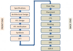
As it shows the design flow starts with a specification document which lists out the technical requirements needed in the chip design. It is followed by translating the specification to Architectural design. The architectural design involves designing the functional blocks and the communication protocol between them and translating them into actual modules that contain FSMs, combinational and sequential circuits etc. The architectural design is then modelled using a Hardware description language like Verilog/VHDL/System Verilog, which is the RTL design stage. The Functional Verification stage starts with a verification plan and a corresponding verification environment which describes and implements the method of proving the design correctness, using different Verification techniques. The design is refined until the HDL model is proved to be meeting the specifications.This stage is followed by Synthesis – a process of transforming the HDL design into a technology specific gate-level netlist, given all the specified constraints and optimization settings. DFT is a structural technique which facilitates a design to become testable after production. All the works till this stage are normally called as the Frontend of VLSI design and are executed by Frontend Engineers.
The next step in the ASIC Design flow is Placement and Routing which involves arranging approximate locations of a set of modules that need to be placed on a layout. Clock tree synthesis is a process which makes sure that the clock gets distributed evenly to all sequential elements in a design to fix the timing violations. This is followed by routing in which exact paths for the interconnection of standard cells and macros and I/O pins are determined.The file produced at the output of the layout is the GDSII (GDS2) file which is the file used by the foundry to fabricate the silicon. Gate level simulations and Static Timing Analysis (a method of validating the timing performance of a design by checking all possible paths for timing violations without having to simulate) are also done to make sure that the gate level design meets the timing requirements for correct design operations. All steps after logic synthesis are performed by Backend engineers and forms the Backend jobs.
Work of a Frontend Engineer
RTL Design/Coding
Synthesis
Functional Verification
DFT
Work of a Backend Engineer
Floor Planning
Placement
Clock Tree Synthesis
STA
Physical Verification
Which one has more career Opportunities?
With the advances being made in technologies like process geometries, feature size and product innovations on a daily basis, there is a constant need to design, develop and re-engineer integrated circuits (ICs). Since electronic products like mobile phones are being released with new features in shorter cycles, there is a healthy demand for qualified VLSI engineers to work on these products. Therefore, there is good scope for a career in the VLSI industry. The important point is that both the domains, front end and back end have their own advantages and have great career prospects. It is completely up to you which one to choose depending on your interest and confidence level, as both offer a great deal of learning and growth.
How to choose?
In order to become a front end engineer, one needs to have good knowledge of HDLs(Verilog/VHDL/SystemVerilog). It will be an added advantage if you have industry related protocol knowledge. So if you have ample digital fundamental knowledge, are fond of HDL coding, love debugging and want to have a sound understanding about the functionality of IC or chip you should definitely go for Front End. With the recent emergence of Artificial intelligence and its application towards VLSI opens up a huge scope for Front end engineers. In order to become a back end engineer, one needs to be well equipped with the concepts of digital electronics, CMOS and Analog Circuits, Scripting knowledge for automation, Hands on Tools for physical design, layout etc. If the above mentioned skills fascinates you then you can opt for Backend and there might be a chance to work in Foundry as well.
Challenges faced by a fresher to get into VLSI industry
Even though VLSI industry is a niche and has lots of career opportunities, on the flip side, industry is currently somewhat less reachable for fresh graduates, compared to other areas due to some particular reasons. Firstly, VLSI or chip design requires a deeper level of knowledge and skills than other electronics related fields .But our Universities are not catering 100% to the VLSI industry requirements. Secondly, VLSI chip design is expensive and requires access to high-cost, specialised electronic design automation (EDA) tools.
How can Chipedge help?
Chipedge offers various courses for fresh graduates both in frontend and backend domains, to choose from. The courses are well structured starting from building a strong foundation by emphasising on fundamental subjects like Digital, CMOS etc. Once the candidate becomes confident with the fundamental knowledge, we impart all the domain specific skills required for the VLSI industry, by giving hands on training on industry standard EDA tools (Synopsys).
1 note
·
View note
Text
Application Specific Integrated Circuits Chip Design Flow

Step 1: Prepare an Requirement Specification
Step 2: Create an Micro-Architecture Document.
Step 3: RTL Design & Development of IP's
Step 4: Functional verification all the IP's/Check whether the RTL is free from Linting Errors/Analyze whether the RTL is Synthesis friendly.
Step 4a: Perform Cycle-based verification(Functional) to verify the protocol behaviour of the RTL
Step 4b: Perform Property Checking , to verify the RTL implementation and the specification understanding is matching. Get More Information Hummer Miner
Step 5: Prepare the Design Constraints file (clock definitions(frequency/uncertainty/jitter),I/O delay definitions, Output pad load definition, Design False/Multicycle-paths) to perform Synthesis, usually called as an SDC synopsys_constraints, specific to synopsys synthesis Tool (design-compiler)
Step 6: To Perform Synthesis for the IP, the inputs to the tool are (library file(for which synthesis needs to be targeted for, which has the functional/timing information available for the standard-cell library and the wire-load models for the wires based on the fanout length of the connectivity), RTL files and the Design Constraint files, So that the Synthesis tool can perform the synthesis of the RTL files and map and optimize to meet the design-constraints requirements. After performing synthesis, as a part of the synthesis flow, need to build scan-chain connectivity based on the DFT(Design for Test) requirement, the synthesis tool (Test-compiler), builds the scan-chain.
7: Check whether the Design is meeting the requirements (Functional/Timing/Area/Power/DFT) after synthesis.
Step 7a: Perform the Netlist-level Power Analysis, to know whether the design is meeting the power targets.
Step 7b: Perform Gate-level Simulation with the Synthesized Netlist to check whether the design is meeting the functional requirements.
Step 7c: Perform Formal-verification between RTL vs Synthesized Netlist to confirm that the synthesis Tool has not altered the functionality.
Step 7d: Perform STA(Static Timing Analysis) with the SDF(Standard Delay Format) file and synthesized netlist file, to check whether the Design is meeting the timing-requirements.
Step 7e: Perform Scan-Tracing , in the DFT tool, to check whether the scan-chain is built based on the DFT requirement.
Step 8: Once the synthesis is performed the synthesized netlist file(VHDL/Verilog format) and the SDC (constraints file) is passed as input files to the Placement and Routing Tool to perform the back-end Actitivities.
Step 9: The next step is the Floor-planning, which means placing the IP's based on the connectivity,placing the memories, Create the Pad-ring, placing the Pads(Signal/power/transfer-cells(to switch voltage domains/Corner pads(proper accessibility for Package routing), meeting the SSN requirements(Simultaneous Switching Noise) that when the high-speed bus is switching that it doesn't create any noise related acitivities, creating an optimised floorplan, where the design meets the utilization targets of the chip.
Step 9a : Release the floor-planned information to the package team, to perform the package feasibility analysis for the pad-ring .
Step 9b: To the placement tool, rows are cut, blockages are created where the tool is prevented from placing the cells, then the physical placement of the cells is performed based on the timing/area requirements.The power-grid is built to meet the power-target's of the Chip .
Step 10: The next step is to perform the Routing., at first the Global routing and Detailed routing, meeting the DRC(Design Rule Check) requirement as per the fabrication requirement.
Step 11: After performing Routing then the routed Verilog netlist, standard-cells LEF/DEF file is taken to the Extraction tool (to extract the parasitics(RLC) values of the chip in the SPEF format(Standard parasitics Exchange Format), and the SPEF file is generated.
Step 12: Check whether the Design is meeting the requirements (Functional/Timing/Area/Power/DFT/DRC/LVS/ERC/ESD/SI/IR-Drop) after Placement and Routing step.
Step 12a: Perform the Routed Netlist-level Power Analysis, to know whether the design has met the power targets.
Step 12b: Perform Gate-level Simulation with the routed Netlist to check whether the design is meeting the functional requirement .
Step 12c: Perform Formal-verification between RTL vs routed Netlist to confirm that the place & route Tool has not altered the functionality.
Step 12d: Perform STA(Static Timing Analysis) with the SPEF file and routed netlist file, to check whether the Design is meeting the timing-requirements.
Step 12e: Perform Scan-Tracing , in the DFT tool, to check whether the scan-chain is built based on the DFT requirement, Peform the Fault-coverage with the DFT tool and Generate the ATPG test-vectors.
Step 12f: Convert the ATPG test-vector to a tester understandable format(WGL)
Step 12g: Perform DRC(Design Rule Check) verification called as Physical-verification, to confirm that the design is meeting the Fabrication requirements.
Step 12h: Perform LVS(layout vs Spice) check, a part of the verification which takes a routed netlist converts to spice (call it SPICE-R) and convert the Synthesized netlist(call it SPICE-S) and compare that the two are matching.
Step 12i : Perform the ERC(Electrical Rule Checking) check, to know that the design is meeting the ERC requirement.
Step 12j: Perform the ESD Check, so that the proper back-to-back diodes are placed and proper guarding is there in case if we have both analog and digital portions in our Chip. We have separate Power and Grounds for both Digital and Analog Portions, to reduce the Substrate-noise.
Step 12k: Perform separate STA(Static Timing Analysis) , to verify that the Signal-integrity of our Chip. To perform this to the STA tool, the routed netlist and SPEF file(parasitics including coupling capacitances values), are fed to the tool. This check is important as the signal-integrity effect can cause cross-talk delay and cross-talk noise effects, and hinder in the functionality/timing aspects of the design.
Step 12l: Perform IR Drop analysis, that the Power-grid is so robust enough to with-stand the static and dynamic power-drops with in the design and the IR-drop is with-in the target limits.
Step 13: Once the routed design is verified for the design constraints, then now the next step is chip-finishing activities (like metal-slotting, placing de-coupling caps).
Step 14: Now the Chip Design is ready to go to the Fabrication unit, release files which the fab can understand, GDS file.
Step 15: After the GDS file is released , perform the LAPO check so that the database released to the fab is correct.
Step 16: Perform the Package wire-bonding, which connects the chip to the Package.
1 note
·
View note
Text
تقنيات جامعية: تصميم دائرة فلب فلوب(S-R Flip Flop) باستخدام لغة الvhdl على برنامج xilinx ise 9.2i
youtube
تهدف لغة VHDL (VHSIC Hardware Description Language) إلى تصميم الأنظمة الإلكترونية الرقمية. تعتبر VHDL من أشهر اللغات المستخدمة في تصميم الأنظمة الرقمية، وتستخدم بشكل واسع في صناعة الدوائر المتكاملة والمنتجات الإلكترونية الأخرى. تم تطوير VHDL في الأصل بواسطة وزارة الدفاع الأمريكية في الثمانينيات، كجزء من مشروع VHSIC (Very High-Speed Integrated Circuit) الذي كان يهدف إلى تطوير تقنيات التصنيع الدقيقة للدوائر المتكاملة. وقد تم نشر نسخة من اللغة للاستخدام العام في عام 1987. تتميز VHDL بقدرتها على وصف التصميم الإلكتروني بشكل دقيق ومفصل، مما يسمح للمصممين بإنشاء نماذج للأنظمة الرقمية واختبارها قبل تصنيعها. تساعد VHDL على تحديد الوظائف التي يجب أن تقوم بها الأجزاء المختلفة من النظام وكيفية تفاعلها مع بعضها البعض. تتكون لغة VHDL من عدة عناصر، بما ��ي ذلك المكونات (components) والعمليات (processes) والإجراءات (procedures) والدوال (functions) والنماذج (models). تستخدم VHDL لوصف الأنظمة الرقمية بشكل هيكلي، مما يسهل فهم تصميم النظام وتحليله. على الرغم من أن VHDL قد تم تصميمها بشكل أساسي لتصميم الأنظمة الرقمية، إلا أنها يمكن استخدامها أيضًا في تصميم الأنظمة الأخرى مثل النظم الميكانيكية والكهروميكانيكية. بشكل عام، تتيح لغة VHDL للمصممين إنشاء نماذج للأنظمة الرقمية وتحليلها وتصحيح الأخطاء قبل تصنيعها، مما يوفر الكثير من الوقت والجهد والتكلفة في عملية التصميم والإنتاج. وتعد VHDL أيضًا مفيدة في توثيق التصميم وتقييمه، حيث يمكن استخدام الشفرة المصدرية لتوثيق تفاصيل التصميم وتحليل الأداء. يتم تنفيذ الأنظمة الرقمية المصممة باستخدام VHDL عن طريق ترجمة الشفرة المصدرية إلى ملفات التصميم القابلة للتصنيع. ويمكن استخدام برامج مختلفة لتحليل وتصحيح التصميم المصمم باستخدام VHDL، مثل Xilinx ISE و ModelSim و Quartus. بشكل عام، تعد VHDL أداة قوية وفعالة في تصميم الأنظمة الرقمية، وهي مفيدة في العديد من الصناعات التقنية. وتحظى بشعبية كبيرة في صناعة الدوائر المتكاملة والإلكترونيات الرقمية والاتصالات والعديد من التطبيقات الأخرى. #xilinx# #ise #9.2i#
0 notes
Text
An Introduction to SystemVerilog: Overview and Benefits
Are you looking to get up to speed with the basics of SystemVerilog? This introduction will provide a comprehensive overview of SystemVerilog and all its benefits. SystemVerilog is an incredibly powerful programming language and hardware description language (HDL) used for the verification, design, synthesis, emulation, and prototyping of digital circuits.
The language enables users to efficiently create intricate designs that can be tested quickly and accurately for verification purposes, as well as optimized for cost reduction when transferred into silicon.
Regardless of your previous experience level or coding expertise, this guide provides all the essentials needed to understand why so many people are drawn towards using SystemVerilog in their projects.
What is SystemVerilog?
SystemVerilog is an extension of Verilog, which was developed by Accellera to enhance the design, verification, and synthesis of digital circuits and systems. This language provides object-oriented programming features, constrained random testing, assertions, and coverage analysis. It has become a popular language for both design and verification of digital systems, due to its flexibility and functionality.
Evolution of Verilog to SystemVerilog
Verilog was enhanced to SystemVerilog to address the growing complexity of digital circuits and systems. SystemVerilog added features such as object-oriented programming, constrained random testing, assertions, and coverage analysis to improve design verification, modeling, and synthesis.
Features and capabilities of SystemVerilog
Some of the notable features and capabilities of SystemVerilog include:
Object-oriented programming (OOP) features, such as classes, objects, and inheritance, enable modular and reusable design structures.
Constrained random testing (CRT) allows designers to create random input stimulus while constraining the values to ensure proper functionality and performance.
Assertions and coverage analysis enable designers to check the correctness of their designs and ensure that they meet the desired functional and performance requirements.
Design hierarchy and interface modeling enable designers to organize and manage complex designs with multiple modules and interfaces.
Design reuse and system-on-chip (SoC) design capabilities facilitate the creation of complex designs with pre-designed components and IP blocks.
SystemVerilog also includes features for low-power design, testbench automation, and FPGA synthesis.
Advantages of SystemVerilog
Here are some advantages of SystemVerilog:
SystemVerilog code is more concise and requires fewer lines of code compared to Verilog, which can save time and reduce errors.SystemVerilog includes structures and enumerated types that provide a more scalable and efficient way to design and manage complex digital systems. Interfaces in SystemVerilog provide a higher level of abstraction and enable faster design iterations and easier reuse of IP blocks.SystemVerilog is widely supported in electronic design automation (EDA) tools, including Vivado synthesis, which makes it easy to synthesize and implement designs on FPGAs
SystemVerilog vs. Verilog
Verilog is a Hardware Description Language (HDL) used for modeling and structuring electronic systems, while SystemVerilog combines HDL and Hardware Verification Language (HVL) to facilitate modeling, designing, simulating, testing, and implementing electrical systems.
In Verilog, module-level testing is used for the testbench, while SystemVerilog utilizes class-level test benches for more advanced and efficient testing. While Verilog uses C and Fortran programming languages, SystemVerilog is a programming language that combines Verilog, VHDL, and C++. Verilog supports the datatypes Wire and Reg, whereas SystemVerilog includes enum, union, struct, string, and class datatypes, enabling more versatile modeling and verification capabilities.
In addition to the differences mentioned earlier, Verilog and SystemVerilog also differ in terms of programming paradigms and procedural blocks.
Verilog supports the structured programming paradigm, whereas SystemVerilog supports both structured and object-oriented programming paradigms, enabling more advanced and modular designs.
In Verilog, there is a single always block to implement both combinational and sequential logic. However, SystemVerilog has three procedural blocks, namely always_comb, always_ff, and always_latch, that provide more precise control over logic implementation.
Verilog is based on a hierarchical module design, while SystemVerilog is based on classes that provide more sophisticated design and verification capabilities.
Conclusion
SystemVerilog is an incredibly powerful and efficient tool for those wishing to develop digital designs quickly and reliably. Its encapsulation of VHDL and Verilog properties in one language makes it a necessary addition to any collection of digital design tools.
The interface options, including the command line, graphical user interface, as well as self-verification facilities will empower users with greater flexibility as well as a sound verification process. With such a comprehensive package, it is no surprise that SystemVerilog has become so popular in the design world.
Get ahead of the game with SystemVerilog today – we at Maven Silicon are here to help you along your learning journey! Whether you’re just starting out or already familiar with SystemVerilog, contact us today to get started on our SystemVerilog tutorial.
With us, by your side, you’ll soon be confident enough to tackle more complex projects with ease. Don't wait - take the first step now and explore what SystemVerilog can do for you!
0 notes
Text
Houston Texas Appliance Parts: How Efinix is Conquering the Hurdle of Hardware Acceleration for Devices at the Edge
Houston Texas Appliance Parts
How Efinix is Conquering the Hurdle of Hardware Acceleration for Devices at the Edge
by Houston Texas Appliance Parts on Tuesday 07 March 2023 08:21 AM UTC-05
In previous articles, we established the many ways FPGAs surpass other AI chipsets for running machine learning algorithms at the edge in terms of reconfigurability, power consumption, size, speed, and cost. Moreover, how the microarchitecture-agnostic RISC-V instruction set architecture (ISA) marries up with the architectural flexibility of the FPGA seamlessly. However, the apparent lack of mid-range, cost-effective FPGAs and their less-than-straightforward design flow are a major bottleneck — the software skills required for the fully custom hardware description language (HDL) implementation are difficult to find and often come with a steep learning curve.
Efinix fills the gap with FPGAs built on the innovative quantum compute fabric made up of reconfigurable tiles known as exchangeable logic and routing (XLR) cells that function as either logic or routing, rethinking the traditional fixed ratio of logic elements (LEs) and routing resources. This allows for a high-density fabric in a small device package where no part of the FPGA is underutilized. The potential of this platform transcends the typical barriers facing edge-based devices today: power consumption, latency, cost, size, and ease of development.
Possibly the most striking feature of Efinix FPGAs is the ecosystem and state-of-the-art tool flow surrounding it that lowers development barriers, allowing designers to readily implement AI at the edge using the same silicon — from prototype to production. Efinix has embraced the RISC-V, thereby allowing users to create applications and algorithms in software — capitalizing on the ease of programmability of this ISA without being bound to proprietary IP cores such as ARM. Since this is all done with flexible FPGA fabric, users can massively accelerate in hardware. Efinix offers support for both low level and more complex custom instruction acceleration. Some of these techniques include the TinyML accelerator and predefined hardware accelerator sockets. With approaches such as these, the leaps in acceleration accomplished delivers hardware performance while retaining a software-defined model that can be iterated and refined without the need to learn VHDL. This results in blazing-fast speeds for edge devices, all while consuming low power and functioning within a small footprint. This article discusses precisely how the Efinix platform simplifies the entire design and development cycle, allowing users to take advantage of the flexible FPGA fabric for a scalable embedded processing solution.
Barriers at the edge — a dam-blocking progress
From massive wireless sensor networks to streaming a high-resolution 360o immersive AR or VR experience, most of the world's data lies at the edge. Disaggregating the compute burden from the cloud and bringing it closer to the devices opens doors for next-generation, bandwidth-hungry, ultra-low-latency applications in autonomous driving, immersive digital experiences, autonomous industrial facilities, telesurgery, and so on. The use cases are endless once the enormous roadblock of transmitting data to and from the cloud is sidestepped.
However, the very defining factors of low-latency, power-hungry compute at the edge are the very same factors that pose a significant design challenge for these small but prolific power-limited devices. How then is it possible to design a device capable of processing the power-hungry relevant ML algorithms without having to invest in elaborate technologies? The solution has been to implement any hardware deemed sufficient to run the suitable applications and algorithms (e.g., CPU, GPU, ASIC, FPGA, ASSP) while accelerating the more compute-intensive tasks to balance the compute time (latency) and resources used (power consumed).
As with any innovation, the landscape of deep learning is continually shifting with updating models and optimization techniques, necessitating the use of more agile hardware platforms that can change almost as rapidly as the programs running on them with little to no risk. The parallel processing and flexibility/reconfigurability of FPGAs seem to line up seamlessly with this need. However, making these devices available for mainstream, high-volume applications requires lowering the design barriers for configuring and accelerating the FPGA fabric — a time-consuming process that normally requires a high degree of expertise. Furthermore, traditional accelerators are typically not granular enough and incorporate large pieces of a model that typically do not scale well. They also generally consume far too much power and are, more often than not, proprietary — causing engineers to relearn how to use the vendor-specific platform.
The Sapphire RISC-V core
Creating an application on the RISC-V Core in C/C++
Efinix squarely addresses all of these potential obstacles by taking on the challenge of making FPGAs available to the AI/ML community in an intuitive way. The RISC-V Sapphire core is fully user configurable through the Efinity GUI; this way, users do not have to know all the VHDL behind implementing the RISC-V in the FPGA and can exploit the straightforward programmability of common software languages (e.g., C/C++). This allows teams to rapidly generate applications and algorithms in software at speed. All the required peripherals and buses can be specified, configured, and instantiated alongside the Sapphire core to deliver a fully configured SoC (Figure 1). This RISC-V capability includes multi-core (up to four cores) support and Linux capability, delivering a high-performance processor cluster to a designer's FPGA application as well as the ability to run applications directly on the Linux operating system. The next step — hardware acceleration — is greatly simplified with hardware-software partitioning; once a designer has perfected their algorithm in software, they can progressively start to accelerate this within the flexible Efinix FPGA fabric. However, before we move on to the next step of hardware acceleration, it would be important to understand the inherent benefits of the RISC-V architecture and how it can be exploited for use within the FPGA fabric.
Figure 1: The Efinity GUI enables designers to configure their Sapphire RISC-V core (left) along with all the required peripherals and buses in familiar programming languages for a fully configured SoC. This capability is extended to up to four RISC-V cores.
Custom-instruction-capable RISC-V
The RISC-V architecture is unique in that it does not have all of its instructions defined; instead, there are a few instructions left open for the designer to define and implement. In other words, a custom arithmetic logic unit (ALU) can be created, and it will perform whatever arbitrary function when called upon by the custom instruction (Figure 2). These custom instructions will have the same architecture as the rest of the instructions (e.g., two registers in, one register out) granting a total of eight bytes of data to work with and four bytes that can be passed back to the RISC-V.
However, since the ALU is built within the FPGA, it can both access and pull data from the FPGA. This allows users to expand beyond the eight bytes of data and make the ALU arbitrarily complex — giving access to data that was put out on the FPGA previously (e.g., access to data from sensors). The ability to have an arbitrarily complex ALU is a multiplying factor for speed when it comes to hardware acceleration. Efinix has taken this ability of the custom instruction and adapted it for the AI and ML communities with the TinyML platform.
Figure 2: Custom ALUs can be created with the RISC-V where the standard configuration includes two source registers (rs1 and rs2) that are four bytes wide and one destination register (rd) that is four bytes wide.
The TinyML platform — a library of custom instructions
Hardware acceleration with the TinyML platform
The TinyML platform streamlines the process of hardware acceleration where Efinix has taken the compute primitives used in TensorFlow Lite models and created custom instructions to optimize their execution on accelerators in the FPGA fabric (Figure 3). Through this, the standard software-defined models of TensorFlow are absorbed into the RISC-V complex and are accelerated to run at hardware speed, taking advantage of the rich, open-source TensorFlow Lite community. The entire development flow has been streamlined using the popular Ashling tool flow to make setup, application creation, and debugging a simple and intuitive process.
Figure 3: TensorFlow Lite creates a quantized version of standard TensorFlow models and uses a library of functions to allow these models to run on MCUs at the edge. Efinix TinyML takes these TensorFlow Lite models, and using the custom instruction capabilities of the RISC-V core, accelerates them in the FPGA hardware.
Many of the TinyML platform's libraries of custom instructions are all available to the open-source community on the Efinix GitHub for free access to the Efinix Sapphire core and everything that is needed to design and develop highly accelerated edge AI applications.
Accelerations strategies: an overview
The combination of the RISC-V core, the Efinix FPGA fabric, and the rich, open-source TensorFlow community allows for creative acceleration strategies that can be broken down into several steps (Figure 4):
Step 1: Run the TensorFlow Lite model using the Efinity RISC-V IDE,
Step 2: Use the TinyML accelerator,
Step 3: User-defined custom instruction accelerator,
Step 4: Hardware accelerator templates.
As stated earlier, "Step 1" is a standard process through the Efinity GUI where users can take the Tensorflow Lite models and run it in software on the RISC-V using the very same, familiar process one would with a standard MCU — without having to worry about VHDL. After Step 1, designers will, more often than not, find that the performance of the algorithm they are running is not optimal and therefore requires acceleration. "Step 2" involves hardware-software partitioning where users can implement the fundamental building blocks inside the TensorFlow Lite models and literally click and drag to instantiate custom instructions and get a massive acceleration on the way the model runs on the Sapphire RISC-V core.
Figure 4: Efinix acceleration strategies.
User-defined custom instruction accelerator
"Step 3" leaves it open for designers to create their own custom instructions without leveraging the templates found in the TinyML platform, allowing users to innovate and create acceleration on top of the RISC-V core.
Hardware accelerator templates
Finally, after the required fundamental elements are now accelerated on the RISC-V, "Step 4" involves burying them inside the free Efinix SoC framework with "sockets" of acceleration. The quantum accelerator socket allows users to "point at" data, retrieve it, and edit its contents to, say, perform a convolution on bigger blocks of data.
The Sapphire SoC can be used to perform overall system control and execute algorithms that are inherently sequential or require flexibility. As stated earlier, the hardware-software codesign allows users to choose whether to perform this compute in the RISC-V processor or in hardware. In this acceleration methodology, the pre-defined hardware accelerator socket is connected to a direct memory access (DMA) controller and an SoC slave interface for data transfer and CPU control, which may be used for pre-processing/post-processing before or after the AI inference. The DMA controller facilitates communication between the external memory and other building blocks in the design by (Figure 5):
Storing frames of data into the external memory,
Sending and receiving data to/from the hardware acceleration block,
Sending data to the post-processing engine.
In an image-signal-processing application, this can look like leaving the RISC-V processor to execute the RGB to grayscale conversion as embedded software, while the hardware accelerator performs Sobel edge detection, binary erosion, and binary dilation in the pipelined, streaming architecture of the FPGA (see "Edge Vision SoC User Guide"). This can be scaled up for multi-camera vision systems, allowing companies to turn their designs into a product and deploy them extremely rapidly.
Figure 5: Sample edge vision SoC framework block diagram.
MediaPipe Face Mesh use case
The simplicity of this process might be better highlighted with an example. The MediaPipe Face Mesh ML model estimates hundreds of different three-dimensional facial landmarks in real-time. Efinix took this model and deployed it on the Titanium Ti60 development kit running at 300 MHz. As shown in Figure 6, convolutions on the RISC-V core contributed the most to latency. It is worth noting that the FPGA's resource utilization of close to 60% does not actually reflect the size of the ML model. Instead, this is due to the fact that the entire camera subsystem has been instantiated in the FPGA in order to perform acceleration benchmarking in real-time.
Figure 6: MediaPipe Face Mesh pre-trained network running on the Ti60 development kit showing both latency and resources used.
Simple custom instructions with the TinyML platform (Step 2)
Creating and running a simple, custom two registers in, one register out convolution instruction shows a four- to five-fold improvement in latency. This improvement continues as custom instructions used to accelerate the ADD, MAXIMUM, and MUL functions. However, latency improvements hit a plateau since the RISC-V is spending less time doing these operations (Figure 7).
Figure 7: Obvious latency improvements with simple, custom instructions created for CONV, ADD, MAXIMUM, and MUL functions.
Complex instructions with DMA (Step 4)
An arbitrarily complex ALU is also generated to replace the original CONV. This changes the slope of the original curve and dramatically improves the latency once more. However, FPGA utilization has also jumped up since the complex instruction has taken more resources inside the FPGA. Once again, the resource bar standing at nearly 100% is simply due the fact that the FPGA here contains the entire camera subsystem for demonstration purposes, what is important to note is the relative decrease in latency and increase in utilization (Figure 8).
What's more, switching to a larger FPGA, such as the Ti180, would run all of these complex instructions for massive acceleration without using even 50 percent of the FPGA resources available. These apparent tradeoffs are precisely what allow engineers to readily visualize the balancing act between latency, power consumption, and the cost/size of the FPGA. An edge application that has stringent latency requirements but more lenient power constraints could opt to increasingly accelerate the design for a drastic performance improvement. In power constrained applications, this increase in performance can be traded off by reducing the clock speed for a more moderate improvement in performance at a dramatically lower power.
Figure 8: A larger custom convolution instruction is employed for much more acceleration; however, resources consumed jumps up. Note, the near full utilization of the FPGA is simply due to the fact that the FPGA contains the entire camera subsystem, this would be dramatically lower if the Ti60 was simply running the ML model
A paradigm shift in AI/ML development
In a nutshell, Efinix has combined the familiar development environment of the RISC-V ISA and exploited its custom instruction capability to function within the architecturally flexible FPGA fabric. Unlike many hardware accelerators, this approach does not require any third-party tools or compilers. The acceleration is also fine grain with the acceleration of machine instructions — a level of granularity that only makes sense with an FPGA.
The fact that edge devices can be prototyped and deployed on the innovative design architecture of the Efinix FPGA means the solution is future-proofed. New models and updated network architectures can be expressed in familiar software environments and accelerated at the custom instruction level with only a small amount of VHDL (with libraries of available templates to use for guidance). This degree of hardware-software partitioning where 90 percent of the model remains in software running on the RISC-V allows for an extremely fast time to market. The combination of all of these approaches yields an elegant solution that truly lowers the barriers to entry for implementing an edge device. Designers now have access to a world-class embedded processing capability that can be accessed with a state-of-the-art tool flow and instantiated on the revolutionary Efinix Quantum fabric.
The post How Efinix is Conquering the Hurdle of Hardware Acceleration for Devices at the Edge appeared first on EE Times.

Pennsylvania Philadelphia PA Philadelphia March 07, 2023 at 08:00AM
Hammond Louisiana Ukiah California Dike Iowa Maryville Missouri Secretary Maryland Winchester Illinois Kinsey Alabama Edmundson Missouri Stevens Village Alaska Haymarket Virginia Newington Virginia Edwards Missouri https://unitedstatesvirtualmail.blogspot.com/2023/03/houston-texas-appliance-parts-how.html March 07, 2023 at 09:38AM Gruver Texas Glens Fork Kentucky Fork South Carolina Astoria Oregon Lac La Belle Wisconsin Pomfret Center Connecticut Nason Illinois Roan Mountain Tennessee https://coloradovirtualmail.blogspot.com/2023/03/houston-texas-appliance-parts-how.html March 07, 2023 at 11:41AM from https://youtu.be/GuUaaPaTlyY March 07, 2023 at 12:47PM
0 notes
Text
Price: [price_with_discount] (as of [price_update_date] - Details) [ad_1] What’s New in the Third Edition, Revised Printing The same great book gets better! This revised printing features all of the original content along with these additional features: • Appendix A (Assemblers, Linkers, and the SPIM Simulator) has been moved from the CD-ROM into the printed book • Corrections and bug fixes Third Edition features New pedagogical features • Understanding Program Performance - Analyzes key performance issues from the programmer’s perspective • Check Yourself Questions - Helps students assess their understanding of key points of a section • Computers In the Real World - Illustrates the diversity of applications of computing technology beyond traditional desktop and servers • For More Practice - Provides students with additional problems they can tackle • In More Depth - Presents new information and challenging exercises for the advanced student New reference features • Highlighted glossary terms and definitions appear on the book page, as bold-faced entries in the index, and as a separate and searchable reference on the CD. • A complete index of the material in the book and on the CD appears in the printed index and the CD includes a fully searchable version of the same index. • Historical Perspectives and Further Readings have been updated and expanded to include the history of software R&D. • CD-Library provides materials collected from the web which directly support the text. In addition to thoroughly updating every aspect of the text to reflect the most current computing technology, the third edition • Uses standard 32-bit MIPS 32 as the primary teaching ISA. • Presents the assembler-to-HLL translations in both C and Java. • Highlights the latest developments in architecture in Real Stuff sections: - Intel IA-32 - Power PC 604 - Google’s PC cluster - Pentium P4 - SPEC CPU2000 benchmark suite for processors - SPEC Web99 benchmark for web servers - EEMBC benchmark for embedded systems - AMD Opteron memory hierarchy - AMD vs. 1A-64 New support for distinct course goals Many of the adopters who have used our book throughout its two editions are refining their courses with a greater hardware or software focus. We have provided new material to support these course goals: New material to support a Hardware Focus • Using logic design conventions • Designing with hardware description languages • Advanced pipelining • Designing with FPGAs • HDL simulators and tutorials • Xilinx CAD tools New material to support a Software Focus • How compilers work • How to optimize compilers • How to implement object oriented languages • MIPS simulator and tutorial • History sections on programming languages, compilers, operating systems and databases On the CD • NEW: Search function to search for content on both the CD-ROM and the printed text • CD-Bars: Full length sections that are introduced in the book and presented on the CD • CD-Appendixes: Appendices B-D • CD-Library: Materials collected from the web which directly support the text • CD-Exercises: For More Practice provides exercises and solutions for self-study • In More Depth presents new information and challenging exercises for the advanced or curious student • Glossary: Terms that are defined in the text are collected in this searchable reference • Further Reading: References are organized by the chapter they support • Software: HDL simulators, MIPS simulators, and FPGA design tools • Tutorials: SPIM, Verilog, and VHDL • Additional Support: Processor Models, Labs, Homeworks, Index covering the book and CD contents Instructor Support Instructor support provided on textbooks.elsevier.com: • Solutions to all the exercises • Figures from the book in a number of formats • Lecture slides prepared by the authors and other instructors • Lecture notes *For the Revised Printing, Appendix A appears in the printed book rather than on the CD. This is the only change.
*Explains the latest benchmarking software including SPEC CPU2000 suite for processors, SPEC Web99 for web servers, and EEMBC for embedded systems *Features the latest developments of the Intel IA-32 architecture as well as the Power PC 604, the AMD Opteron Memory, and the Intrinsity FastMATH processor. *Compares MIPs assembler code to both C and Java ASIN : 0123706068 Publisher : Morgan Kaufmann; 3rd edition (27 July 2007); CBS PUBLISHERS & DISTRIBUTORS PVT. LTD 01149349337 Language : English Paperback : 741 pages ISBN-10 : 9780123706065 ISBN-13 : 978-0123706065 Item Weight : 1 kg 340 g Dimensions : 19.69 x 3.18 x 22.86 cm Country of Origin : India Net Quantity : 1 Count Importer : CBS PUBLISHERS AND DSITRIBUTORS PVT LTD PHONE-01149344934 Packer : CBS PUBLISHERS AND DISTRIBUTORS PVT LTD PH: 011-49344934 Generic Name : Textbook [ad_2]
0 notes